ASML’s $400M High-NA EUV Machine Will Produce Its First Chips Within Months — Here’s Why It Changes AI Forever
Table of Contents
Table of Contents
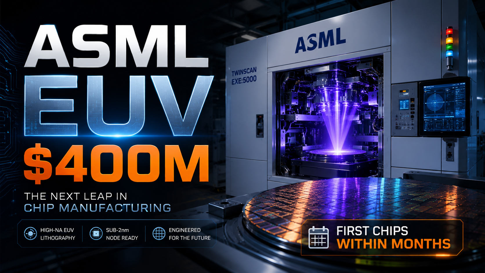
The most powerful chipmaking machine ever built — a device that costs $400 million, weighs 180 tonnes, and requires a Boeing 747 to ship — is about to start producing the chips that will power the next generation of AI. ASML CEO Christophe Fouquet announced on May 19, 2026 that the first commercial chips manufactured using its High-NA EUV lithography technology are expected to emerge “within months.” This is the moment the semiconductor industry has been anticipating for over a decade — and it has enormous implications for the global AI arms race.
What Is High-NA EUV — And Why Does It Matter?
EUV stands for Extreme Ultraviolet lithography — the process ASML uses to etch circuit patterns onto silicon wafers using light with a wavelength of just 13.5 nanometers. “High-NA” refers to a higher numerical aperture (0.55 vs. the standard 0.33), which allows the machine to focus light more precisely, producing finer chip features.
In practical terms: High-NA EUV can print circuit features as small as 8 nanometers, compared to the roughly 13nm achievable with standard EUV. That may sound like a minor difference, but in chip physics it means dramatically more transistors packed into the same space — translating directly into faster processing, lower power consumption, and more capable AI.
ASML’s High-NA EUV machine, the EXE:5000, is literally the most complex manufacturing device ever built by humans. It contains over 100,000 components, requires a dedicated team of engineers just to operate, and can only be manufactured at ASML’s facility in Veldhoven, Netherlands — making the Dutch company one of the most strategically critical corporations on Earth.
From Lab to Factory: The Timeline
ASML has been shipping High-NA EUV machines to customers — primarily Intel and Samsung — since late 2025. But shipping a machine and producing commercial chips with it are very different things. The machines require months of calibration, facility preparation, and process development before they can be used for mass production.
CEO Fouquet’s May 19 statement that chips are “within months” away represents the transition from engineering development to commercial production readiness. The first volume chips are expected to appear in consumer and enterprise products by late 2026 or early 2027 at the earliest, though initial volumes will be small and expensive.
ASML is ramping production of EUV systems broadly: the company plans to deliver at least 60 EUV systems in 2026, up 20% from the 48 delivered in 2025. High-NA units represent a small fraction of that total, but demand is growing rapidly.
Intel vs. TSMC: Diverging Strategies
The two dominant chipmakers are taking starkly different approaches to High-NA EUV:
Intel is betting heavily on High-NA EUV as its path back to manufacturing leadership. After years of struggling to keep pace with TSMC, Intel sees first-mover advantage on the new technology as its best chance to regain its footing. Intel’s 18A process node — the first designed with High-NA EUV in mind — is at the center of its 2026 comeback strategy.
TSMC, by contrast, has deliberately chosen not to use High-NA EUV in its near-term processes. TSMC’s latest process nodes use existing EUV machines but apply more exposure passes (“multi-patterning”) to achieve comparable resolution. TSMC’s argument: maximize what works reliably rather than take on the risks of a new, extremely expensive technology.
Both strategies have merit. Intel needs a leap to catch up. TSMC is protecting its position as the world’s most reliable mass-production chipmaker. The real test will come in 18-24 months when both approaches produce yield data at volume.
The Geopolitical Dimension: Why One Dutch Company Controls the Future
ASML holds a complete global monopoly on EUV lithography. No other company on Earth can build these machines. This gives the Netherlands — and by extension, the European Union and the US (which pressured the Netherlands to restrict ASML exports) — extraordinary leverage over which countries can build advanced chips.
China has been completely cut off from ASML’s EUV equipment since 2023, and the restrictions have since extended to some of ASML’s older DUV (Deep UV) machines as well. Chinese chipmakers like SMIC are stuck at 7nm or above — multiple generations behind where High-NA EUV is heading. This is why China is investing billions in domestic lithography alternatives, but analysts don’t expect them to reach High-NA EUV capability for at least another decade.
The semiconductor equipment control battle is arguably more consequential than the chip tariffs and trade wars making headlines. As the AI chip race intensifies and companies like Cerebras push performance boundaries, access to next-generation chipmaking tools will determine which nations can independently develop advanced AI — and which cannot.
What This Means for AI: More Power, Less Energy
Every major AI trend right now runs into the same wall: compute. Training large language models, running inference at scale, powering models like Gemini 3.5 and GPT-5 — all of it requires chips that are faster, more power-efficient, and more densely packed than what exists today.
High-NA EUV chips will deliver:
- Higher transistor density — more compute per square millimeter of silicon
- Lower power consumption per operation — critical for data centers already straining power grids
- Better performance-per-watt — enabling AI capabilities previously impossible at current energy costs
- Smaller form factor — enabling more powerful AI in edge devices, phones, and eventually wearables like the Android XR glasses Google just announced
The AI companies spending hundreds of billions on infrastructure — including Meta’s $135 billion 2026 capex — are betting that High-NA EUV chips will dramatically improve the economics of AI compute. If they’re right, the ROI on today’s massive AI infrastructure investments becomes much more plausible.
The Challenges: Cost, Yield, and Supply
High-NA EUV isn’t without risks. The key challenges:
- Cost per chip — The machines are so expensive that the cost per wafer is dramatically higher than existing EUV, at least in early production runs. Yield improvements over time will lower costs, but initial chips will be priced at a significant premium.
- Resist chemistry — High-NA EUV requires new photoresist materials that don’t exist yet at production scale. Material suppliers are racing to keep up.
- Pellicle availability — Protective membranes (pellicles) for High-NA EUV masks are critical but still in limited supply, potentially bottlenecking production ramp.
- Single-source risk — If anything goes wrong at ASML’s Veldhoven facility, there is no alternative supplier. The world’s chip supply depends on one factory in one city in one country.
Bottom Line: A New Era of Chips Is Weeks Away
ASML’s announcement on May 19 is one of those quiet inflection points that doesn’t make front-page news but reshapes the world. The $400 million machines sitting in Intel’s and Samsung’s fabs are about to start producing chips that will power the next 10 years of AI development.
For the AI industry, this is as fundamental as electricity getting cheaper. For China, it’s a widening gap that’s becoming harder to close. For ASML, it’s vindication of a decades-long technology bet that most people said couldn’t be done.
The chips are coming. And they’re going to change everything — again.